|
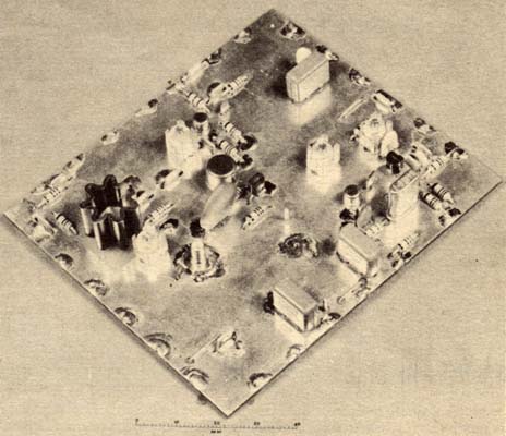
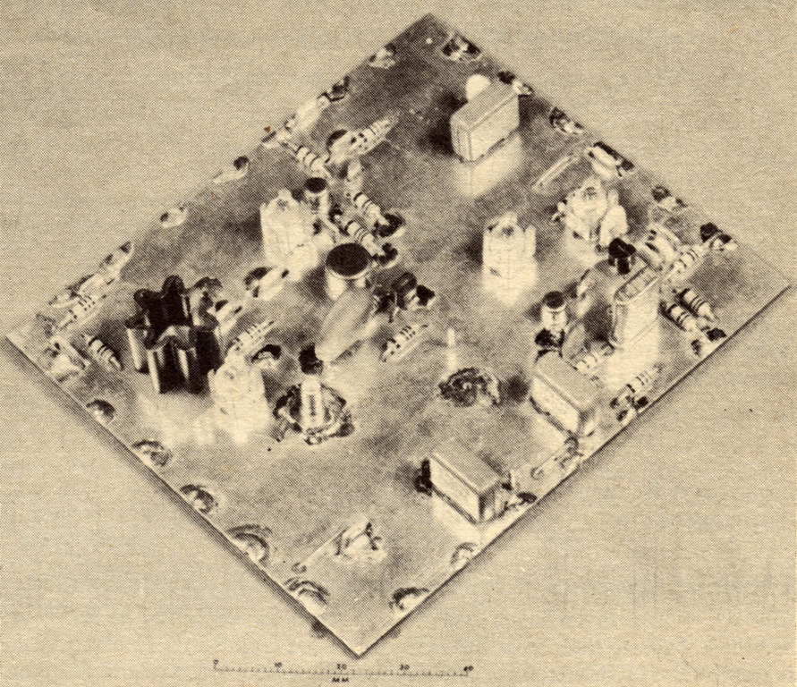
The completed source board.
This article was published in the October 1981 edition of the RSGB magazine RadCom. This design was, for a number of years, the definitive oscillator board for the generation of signals for multiplying up to the microwave bands.
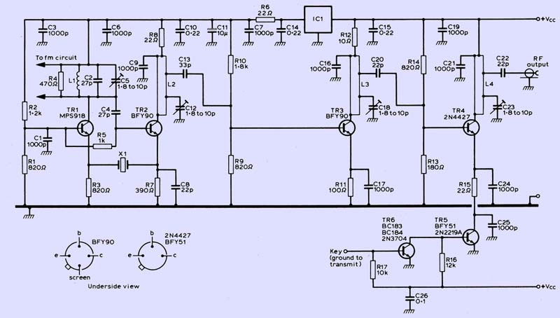
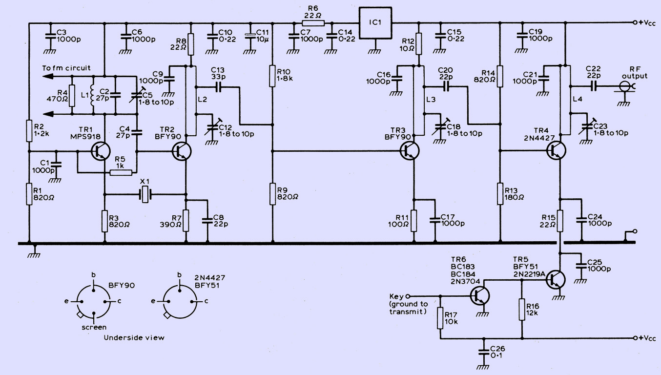
The circuit diagram.
Introduction
This article describes a unit to deliver a minimum of l00mW from a 12V supply, at an output frequency of 360-440MHz, using a fifth overtone crystal in a range 90-11OMHz. Its output is intended for multiplication up to microwave frequencies for use as a local oscillator or transmitter, and still has a good quality note at 10GHz. It has been developed by members of the RSGB Microwave Committee from the Plessey AMETS transmitter board.
The design uses a Butler crystal oscillator, which eliminates frequency multiplier stages and gives a very-low-noise output compared with the commonly-used single-transistor circuits. This is due to the loading on the crystal being less, thus allowing a higher working Q to be realized.
Leadless disc capacitors are used on a double-sided pcb for efficient decoupling, and the two amplifier stages are run in Class A, contributing to the low-noise performance and making problems with instability very unlikely. All inductors and lines are printed on the board, and only four adjustments are needed to align the unit. Provision is made for on/off keying of the output stage, or for applying FM or FSK to the oscillator. Several dozen of these boards have been built and used in a variety of microwave applications, giving excellent results.
Construction
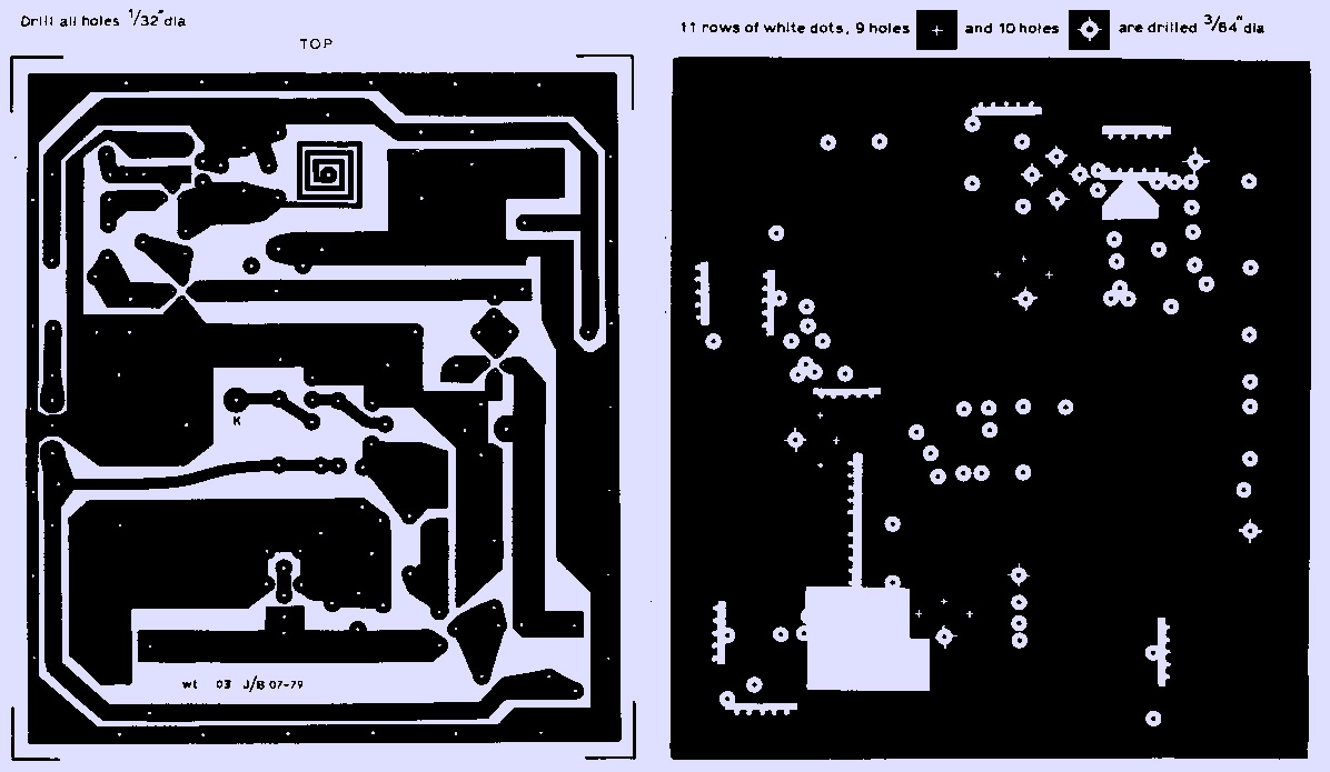
The unit is constructed on 0.063in (1.59mm) thick double-sided copper-clad glass-fibre epoxy board (dielectric constant approx equal to 5) with an earth plane on the component side of the board. The use of materials with different dielectric constants could result in incorrect resonant frequencies for the tuned circuits, and should be avoided. The circuit diagram is given above, and the artwork for the two sides of the pcb is shown in below.
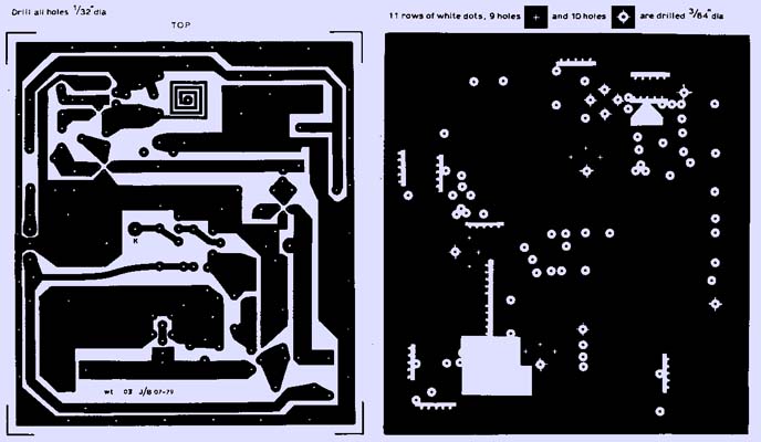
The board artwork.
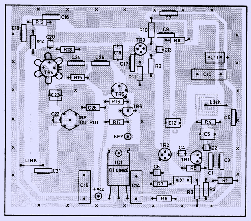
Construction is generally straightforward; the layout of components on the pcb is shown below. It is important that the component values are adhered to, and in particular that only new, branded semiconductors are used for TR1-4. Surplus types do not usually perform satisfactorily. The earthed ends of the components are soldered to both top and bottom earth planes, and all components should be mounted with absolute minimum lead lengths. TR2, TR3 and TR4 should be pushed right down on to the top side of the board, and the cans of TR2 and TR3 soldered to the earth plane. TR4 is fitted with a TO5 heatsink.
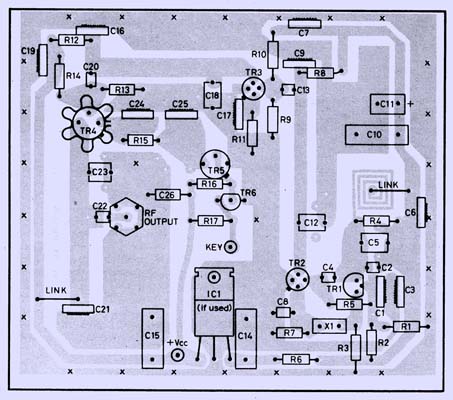
The component positions. An x indicates worm joining top and bottom earth planes.
Care should be taken in the mounting of the 1,000pF leadless disc ceramic capacitors. They are located in slots in the pcb made by drilling several holes close together and then joining them to form a slot. This can be done quite easily using the tool shown below, which is made by taking a junior hacksaw blade, breaking off the end with the pin through it, and cutting or filing the end to a taper. The teeth should be oriented as shown. The point is thin enough to fit into one hole at the end of the row and enable it to be opened up, and then the remaining holes can be joined up progressively.
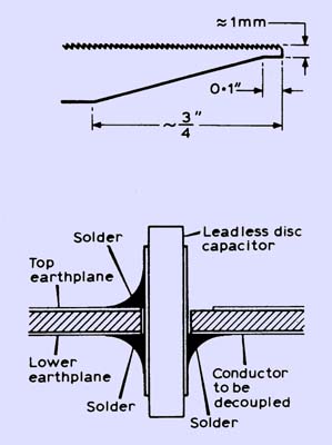
Mounting process for 1,000 pf leadless capacitors.
The hacksaw blade must be held quite close to the board, and used gently to start with to prevent it snapping off; if it does, it can easily be repaired by filing it to a point again. Another method is to use a 1mm drill bit in a vertical drill as a mill. Hold the drill bit in the chuck so only 3 or 4mm protrude, and move the board sideways so that the edge of the drill bit cuts the slot, joining the holes. Hold the board against a straight edge to ensure a straight slot, if the drill breaks, it can still be reused. The edges of the slot can then be cleaned up with a flat needle file or nail file. Do not make the slot too wide, otherwise it will be difficult to solder the discs, which should be positioned and soldered exactly as shown above. Ensure that the solder flows properly on to the metallization on the capacitors. Various 'surplus' leadless discs gave trouble in this respect on some of the prototypes, and the most reliable types were found to be those made by Steatite[1] which are actually trapezoidal (coffin-shaped) rather than round. They proved extremely easy to solder in place, and are thoroughly recommended.
For other types, a useful technique is to heat the edge of the slot first, insert the disc, apply the soldering iron to the disc (not the board), and then apply solder to form a neat fillet. If silver-loaded solder can be obtained, then this is also worth using.
The earth planes on both sides of the board are joined at many points by wire 'worms' which are short lengths of 20-24swg wire (eg scrap component leads) soldered in all the remaining holes that are not cleared on the upper side of the board. These are located all round the edge of the board, as well as in a number of other places. It would be possible to replace the worms round the edges of the board by some thin copper foil, folded and soldered along the edges of the board, connecting the two earth planes. Do not forget the two wire links on the board connecting L1 and L4 to the positive supply. Holes are provided for either the 2- or 3-pin types of trimmer capacitor, which should be mounted so that their movable vanes are connected to the earthy side of the tuned circuits to minimize stray capacitance coupling and loading effects when trimming tools are used.
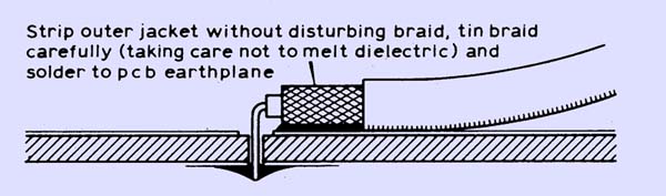
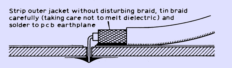
The mounting of co-axial cable for direct take-off of the output.
The output can be taken either by small-diameter coaxial cable directly from the board, with the cable outer soldered carefully to the top earthplane, or from an SMB, SMC (Conhex) or SMA socket on the board.
Provision has been made on the board for a TO220 voltage regulator for the oscillator supply, which reduces the chirp on the note considerably if the board is to be A1 keyed. These regulators generally require an input voltage at least 2.5V greater than the regulated output voltage, so if a 12V one is used (eg 7812, LM340TI2), the supply to the board should be at least 14.4V. If only a 12V supply is available, as would usually be the case when operating portable, either use an 8V regulator (7808) - though this may reduce the output slightly - or omit the regulator altogether and insert a wire link between the two outermost regulator holes.
Modulation facilities
The pa stage can be on/ off keyed by TRS and TR6. However, this pulls the oscillator frequency slightly, and the keying chirp at 10GHz is unacceptable unless the oscillator voltage regulator (ICI) is used, and even then it is still noticeable. Frequency shift keying is the preferred method of keying. If the A1 keying facility is not required, TRS, TR6 and their associated components should be omitted, and the end of R15 previously connected to TR5 grounded directly.
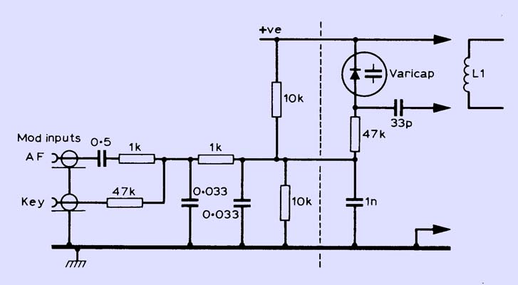
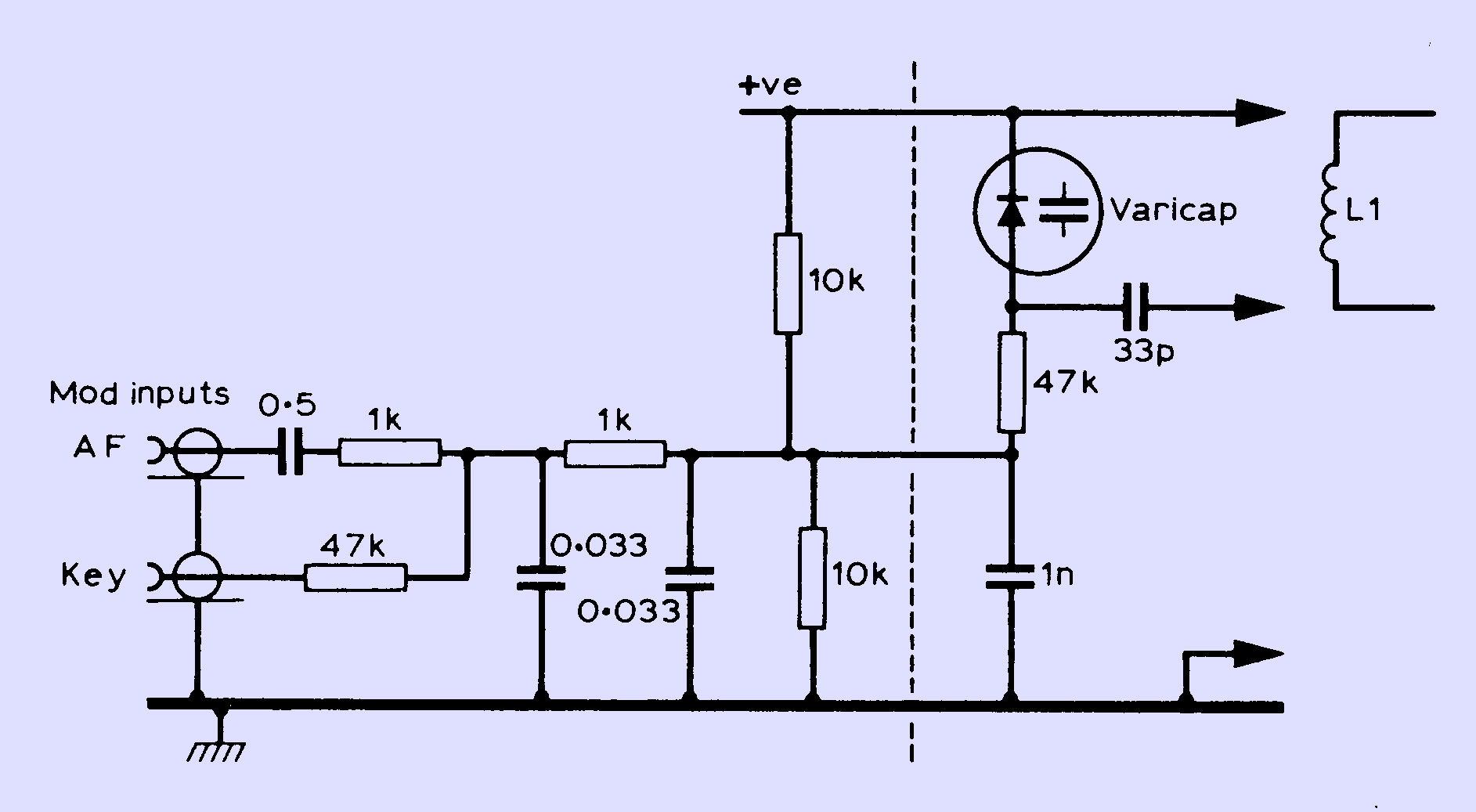
Network for FM and FSK modulation.
Frequency modulation or fsk can be produced using the circuit above in which a varicap diode varies the capacitance across L1. The value of C2 must then be reduced to maintain the total capacitance at 27pF. The BBI05B (C=7pF at -5V) with C2=18pF should give a deviation of about 2kHz/V at 10GHz. Wider deviation could be obtained by using a higher capacitance diode such as the BB110G, or a hyper-abrupt type which has a larger capacitance swing, eg the Alpha DKV6520 [6].
Inputs are provided for audio at low impedance (source impedance less than 1k Ohms), or CW where earthing the input shifts the carrier about 1kHz HF at 10GHz; the shift can be altered by changing the 47k Ohm resistor.
The components to the right-hand side of the dotted line should be mounted directly across the tuned circuit. The rest can be mounted in place of the A1 keying circuit if this is not required, but in any case they should be mounted on the board to avoid earth loop problems. Efficient filtering is necessary on both inputs to prevent any stray AF or RF noise causing unwanted sidebands on the output.
Alignment
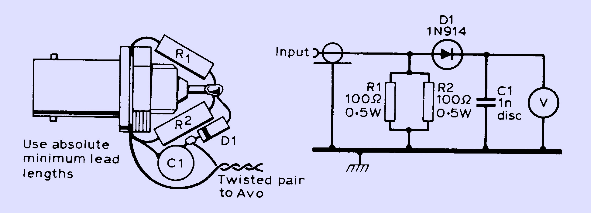
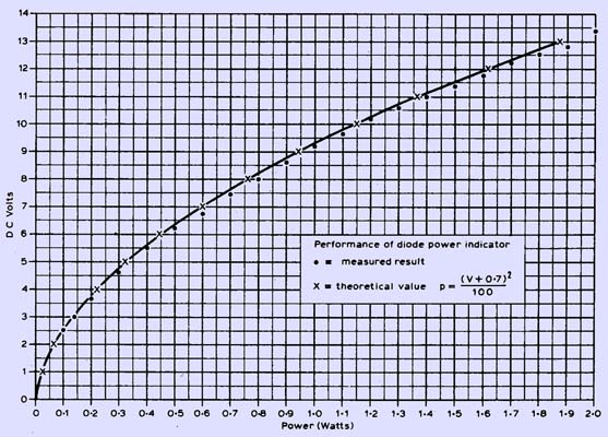
The tuning-up procedure for this board requires the use of some form of output indicator. An HF/VHF SWR meter connected to the board via a short length of coaxial cable can be used, set initially on its most sensitive range,and with a 50 Ohm load or resistor on its output socket. It is recommended, however, that the power meter described below is used, as it is a simple, yet remarkably accurate way of measuring power in the range l00mW to 2W, up to at least 500MHz.
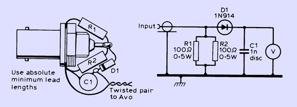
Construction of the power meter on a BNC socket.
Construction details are given above. The meter indication, V, is the peak RF voltage across the load minus the forward voltage drop across the diode. This is divided by root 2 to give the RMS value, and the power is calculated from this using the equation.
P = (Vrms)*2 / R
For germanium diodes, such as the OA47, the relationship will thereforebe
P = (V + 0.25)*2 / 100
while for silicon diodes, such as 1N914, 1N916, 1N4149, it is
P = (V + O.7)*2 / 100
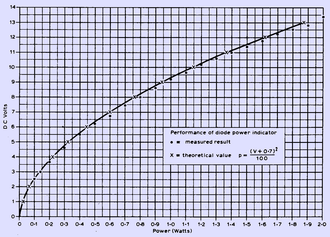
The results from this meter using a 1N914 at 500MHz are compared with the actual power below
Power meter performance.
and show the high accuracy obtainable. Apply power to the board, and check the current drawn (approximately 150mA). For a 96MHz crystal, preset the trimmers to the following positions: C5 about 50 per cent meshed, C12 about 40 per cent meshed, C18 about 80 per cent meshed and C23 about 50 per cent meshed. Some output should be detected, and this is maximized by peaking the trimmers.
It should not be possible to tune up on the wrong frequency using the component values specified, but if in doubt check with an absorption wavemeter. The position of C5 should not be too critical as regards output power, and may be used to trim the frequency. If crystal frequencies outside the range 90-100MHz are used it may be necessary to alter the value of C2 so that as C5 is adjusted over about half its travel, the power output stays constant but the frequency pulls smoothly. If necessary the frequency can be raised slightly by putting a 5-20pF trimmer in series with the crystal, but this may reduce the power output or stability, and in general it is preferable to put up with a small frequency offset (which can be calibrated out) rather than compromise on stability.
When the board is tuned up it should produce a comfortable 100mW RF output. It may be possible to increase this slightly by optimizing certain components (eg R10, C8, C22) but if more power is needed it is preferable to add an extra stage, rather than risk detracting from the stability, low noise sidebands and reliability of the oscillatorboard.
Decoupling, screening and supply regulation
The board is designed to fit in an STC (ITT) 116 x 90mm diecast box (part number 46R CS00 043 A00) with the internal ribs filed away to fit. The board should be mounted, by bolts in its corners, about 5mm off the bottom of the box to avoid excessive damping of the lines by the box, and to ensure that the heatsink on TR4 does not touch the lid of the box. This, or similar screening, is recommended for best results, as any feedback from subsequent stages to the oscillator can degrade the note. Whatever type of power supply is used, it is essential to prevent any RF or AF noise from reaching the board on the supply, as this can cause either a noisy carrier, or sidebands on the output, so all connections, eg supply, keying etc, must be thoroughly decoupled. A feedthrough where the leads pass through the box, with a small 10-100μH RFC outside the box, in series with the supply, should be adequate, although a Filtercon is preferable. If possible check with a wide-bandwidth oscilloscope that any voltage regulator circuits are not oscillating-possibly at quite a low level. This can occur at anywhere from audio to tens of megahertz.
The board should be earthed to the box at several places, and the lid should be screwed firmly in place, as any intermittent contact here may cause jumps in frequency. The outer conductor of the RF output should be earthed where it passes through the box, eg by mounting a socket on the box. In general the amount of effort that must be put into these precautions depends upon the factor by which the frequency is to be multiplied.
The on-board regulator, IC1, is probably only worth using if it is intended to use the A1 keying facility, or if a +15V supply is available. Without the regulator the board will operate satisfactorily from a supply as low as 11V, with little drop in output.
For best frequency stability the whole board must run from a stabilized supply, and it is desirable that this should be the same voltage whether for portable or fixed operation, so that the frequency calibration is maintained. This is particularly important when using car batteries, as their voltage varies somewhat according to the state of charge, current drawn, etc. (perhaps as much as 11.5V to 16V), and the same is true of some other types of battery.

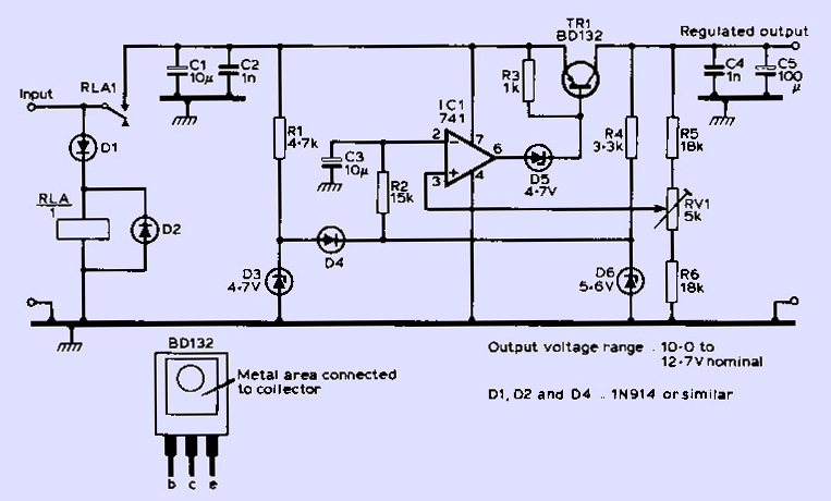
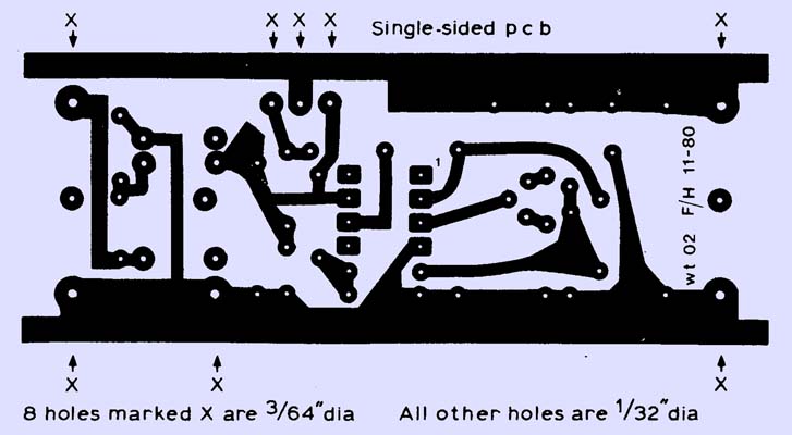
Low voltage-drop regulator.
The circuit shown above makes the oscillator well and truly insensitive to supply voltage variations, and provides over-voltage and reverse supply protection. It will regulate down to a minimum voltage drop of approximately 300mV (governed by the Vce sat of the transistor). A pcb design is given, and the board layout is presented below.

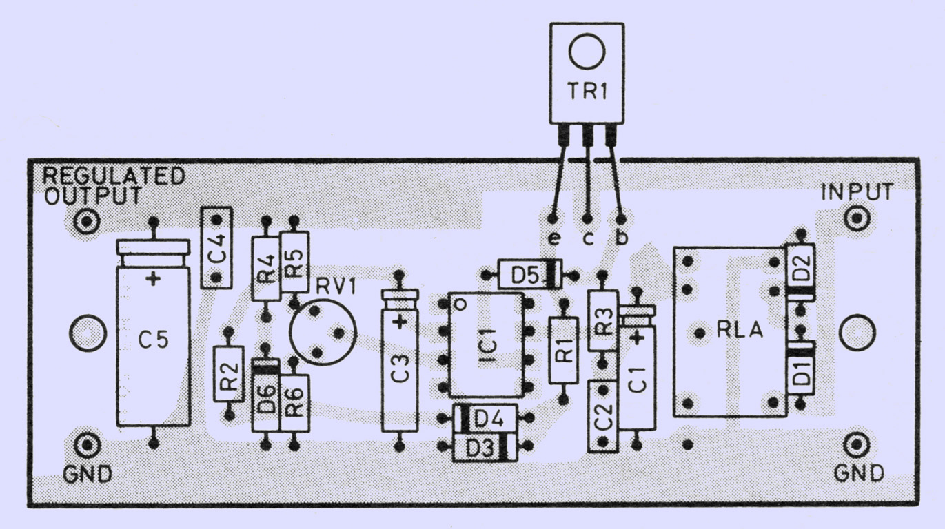
Component layout for low-voltage drop regulator.
The relay used for reverse supply protection (Radiospares 348-510) is rated at 1A 28V, so this circuit can be used (and is highly recommended) for all pieces of gear that need a regulated supply up to this rating, and arelikely to be used portable. RV1 sets the regulated output voltage;something like 11.2V is suggested as a reasonable value that will guarantee a regulated output even at the lowest supply voltages. The BD132 transistor is bolted to a suitable heatsink, with the usual insulating washer.
Regulator board track artwork.
Performance
The following results give typical performance figures measured on the board shown in the photograph.
Supply voltage (V) | Output power (mW) |
11.0 | 225 |
12.0 | 270 |
13.5 | 325 |
15.0 (without IC1) | 350 |
15.0 (with IC1) | 350 |
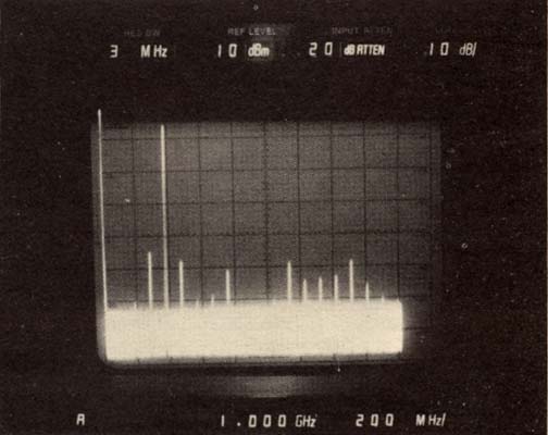
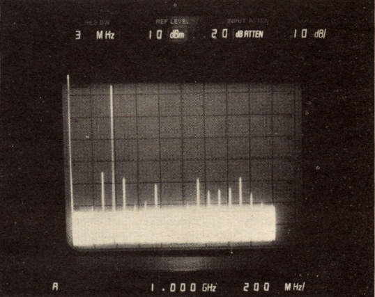
Spectrum analyser performance.
The spectrum of the output is shown above. This varies very little with supply voltage. Unwanted products are better than 35dB down on the main carrier.
Frequency stability (at 10GHz)
Variation of frequency with supply voltage: without IC1, -5kHz/V; with IC1 -100Hz/V (once regulating); with voltage-drop regulator, hardly detectable.
Variation of frequency with temperature: 2kHz/°C (this depends somewhat on the crystal)
Applications
Most of the boards that have been built so far have been used on 10GHz to provide a local oscillator for the G3JVL 10GHz transverter [2] in conjunction with the GSDEK step-recovery multiplier design [3]. Most of the comments in this article refer to measures required to give a good note at this frequency. For this application a 94.666MHz crystal is used to give an output at 378.666MHz, for a final local oscillator frequency of 10.224GHz. An output power of about 2.5W is needed, so some form of additional amplifier is required. This should not be mounted in the same box as the board.
RF output frequencies and crystal frequencies for various applications of the board
Application | RF output frequency (MHz) | Crystal frequency (MHz) |
Microwave CW/FSK/FM tx | 384 | 96 |
1.3 GHz Converter/transverter (144 MHz IF) | 384 | 96 |
2.3 GHz Converter/transverter (144 MHz IF) | 360 | 90 |
3.4 GHz Converter/transverter (144 MHz IF) | 368 |
5.7 GHz Converter/transverter (144 MHz IF) | 374.4 | 93.6 |
10 GHz Converter/transverter (144 MHz IF) | 378.666 | 94.666 |
24 GHz Converter/transverter (144 MHz IF) | 95.4286 |
Amplifiers that have been used with success for this include the Mullard BGY22 module (which requires an attenuator [4] at its input to reduce the power from the board to approximately 50mW) and the Wood & DouglasMD3PA. While the former is very simple and convenient, the latter has rather better spectral purity. The Mullard BGY22/BGY23 combination or the Wood & Douglas MD10PA [5] are also recommended as higher power amplifiers for transmitter-type applications.
Crystal frequencies and RF output frequencies for various applicationsare given below.
Conclusion
Although the board is quite simple to construct and align, there is no compromise in performance. Its versatility should eliminate all problems of building a new local oscillator strip design for each new microwave project.
References
- Steatite-Roederstein Ltd, Hagley House, Hagley Road, Birmingham B16 8QW. (Note: #50 minimum order charge, G3YGF has agreed to keep a stock of both these leadless discs and also the ready drilled pcbs.)
- G3JVL IOGHz Transverter, RadCom January and April 1979, pp41, 342, April 1980, pp372-5, February 1981, pl46.
- G8DEK BXY41E 10GHz step-recovery diode multiplier, RadCom March 1976, p202
- Design and construction of simple attenuators RadCom March 1979, p239
- Equipment review - Wood & Douglas 384MHz MDO5T microwave drive source and MDIOPA power amplif1er kits. RadCom June/July 1980, pp 650-2.
- Alpha Industries, RMC House, Station Road, Witney, Oxon OX8 6BP
|